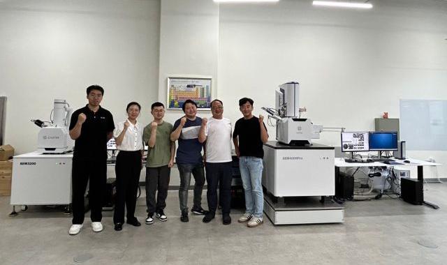
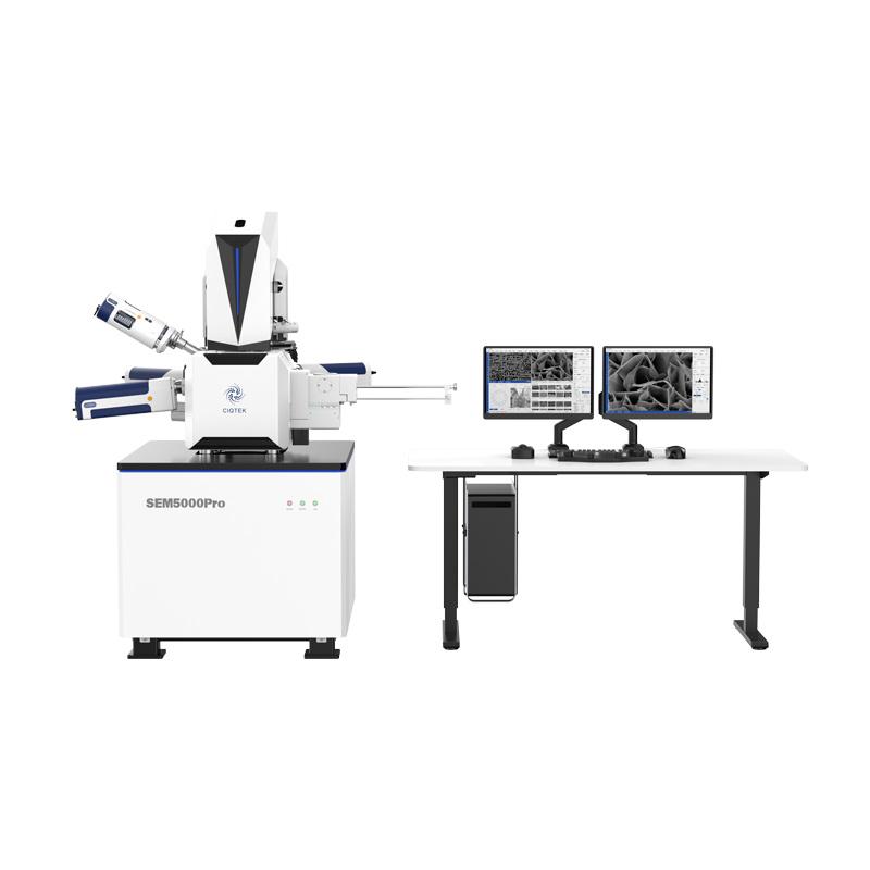
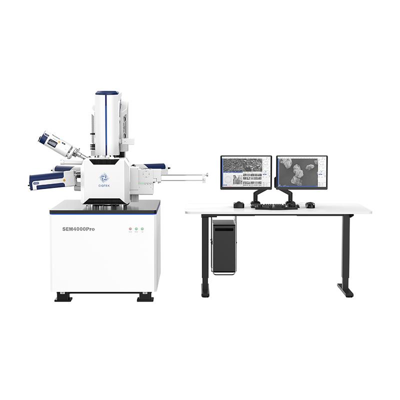
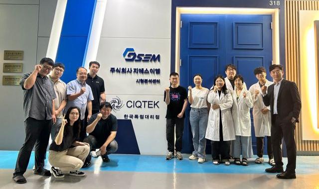
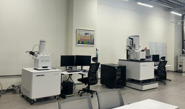
Suwon, Korea - In a significant development, leading scientific equipment distributor GSEM Korea has successfully installed cutting-edge SEM3200 and SEM4000Pro Scanning Electron Microscope (SEM) at its testing center in Korea.

 GSEM Korea has successfully installed cutting-edge SEM3200 and SEM4000Pro Scanning Electron Microscope (SEM) at its testing center in Korea

The SEM3200 and SEM4000Pro SEM Microscope of CIQTEK represent a breakthrough in modern high-resolution imaging. With advanced electron microscopy technology, these cutting-edge SEM Microscopes will provide exceptional tools and platforms for Korean researchers and industry professionals, driving advancements in various fields.

GSEM Korea has successfully installed cutting-edge SEM3200 and SEM4000Pro Scanning Electron Microscope (SEM) at its testing center in Korea 

"We are thrilled with the installation of the SEM3200 and SEM4000Pro," said a research scientist at GSEM. "The high resolution and advanced imaging capabilities allow us to gain valuable insights into microscopic analysis, enabling us to optimize and tailor their performance for specific applications. "

 GSEM Korea has successfully installed cutting-edge SEM3200 and SEM4000Pro Scanning Electron Microscope (SEM) at its testing center in Korea

With an extensive sales network and a dedicated team of technical expertsGSEM remains committed to fostering scientific innovation and progress, providing excellent instrumentation, and delivering technical support for researchers and industry professionals in Korea. They collaborate with businesses and research institutions to drive the development of scientific research, making significant contributions to Korea's innovation and sustainable growth.


Microscopy has revolutionized our understanding of the microscopic world, enabling scientists to reveal complex structures and study materials at the nanoscale. Among the various powerful microscopes, the scanning electron microscope (SEM) is an indispensable tool for imaging surfaces with extraordinary detail and resolution.

In this blog post, we will look in-depth at different types of scanning electron microscopes and explore their unique capabilities and applications.


Conventional Scanning Electron Microscope (C-SEM)

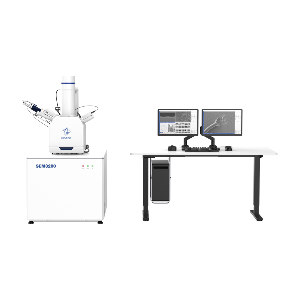
A conventional scanning electron microscope, also known as a single-beam scanning electron microscope, is the most common type. It consists of an electron source that generates a high-energy electron beam, which is focused and scanned over the surface of a specimen. An electron detector captures the resulting signal and constructs a high-resolution image. The C-SEM is a versatile instrument capable of imaging a wide range of samples, including biological samples, materials, and semiconductor devices.

CIQTEK C-SEM Tungsten Filament SEM - SEM3200Check CIQTEK C-SEM Tungsten Filament SEM - SEM3200


Environmental Scanning Electron Microscope (ESEM)

Designed to analyze samples in their natural or hydrated state, environmental scanning electron microscopes are therefore suitable for studying fragile or aqueous samples. Unlike C-SEM, ESEM can image under different pressure conditions without the need for extensive sample preparation. This type of scanning electron microscope is particularly suitable for life sciences, geology, and environmental studies.


Field Emission Scanning Electron Microscope (FE-SEM)

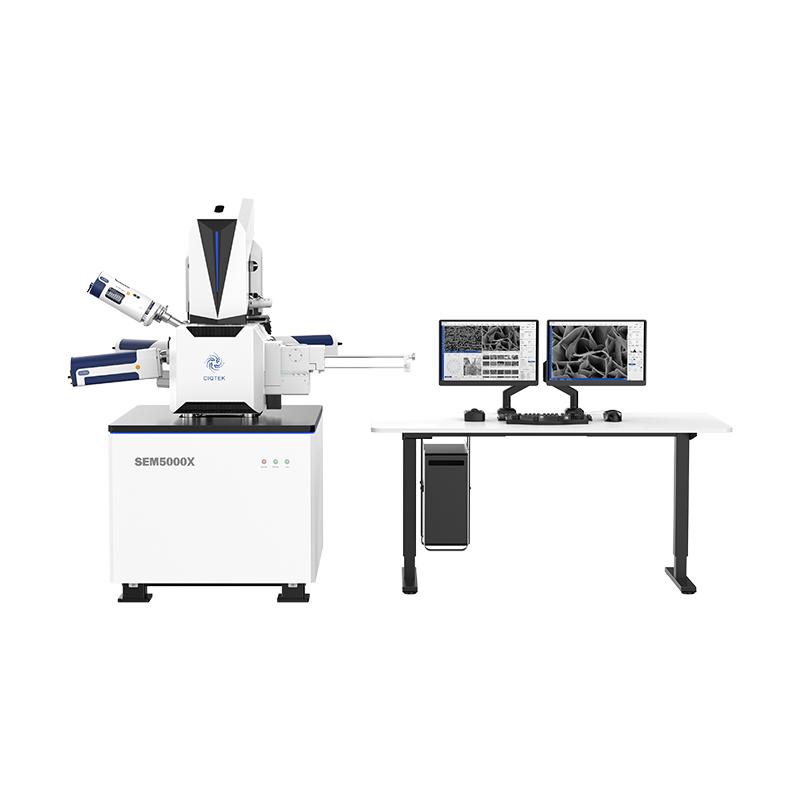
Field Emission Scanning Electron Microscopes utilize field emitters as an electron source to produce electron beams of incredible intensity, resulting in improved resolution and signal detection. With atomic-level resolution, FE-SEMs are ideal for examining advanced materials, analyzing nanoparticles, and studying nanoscale structures. They have applications in materials science, nanotechnology, and semiconductor research.

Check CIQTEK Ultra-high Resolution FESEM - SEM5000X

fesem edxfield emission scanning electron microscopyfield emission scanning electron microscope fe sem


Low-Voltage Scanning Electron Microscopy (LV-SEM)

LV-SEMs operate at relatively low voltages compared to C-SEMs, which provides a distinct advantage for imaging non-conductive or beam-sensitive materials. By operating at lower voltages, LV-SEM minimizes damage to the sample and enhances imaging of insulated samples without the need for conductive coatings.LV-SEM can be applied to biological research, polymers, and poorly conductive materials.


Variable Pressure Scanning Electron Microscopy (VP-SEM)

Variable Pressure Scanning Electron Microscopy combines the capabilities of a conventional scanning electron microscope and an ambient scanning electron microscope to image samples that have limited vacuum compatibility or are susceptible to surface charging. By introducing gas into the scanning electron microscope chamber, VP-SEMs mitigate charging effects and provide high-resolution imaging of non-conductive materials. This makes them suitable for applications in forensic science, archaeology, and art conservation.


Scanning electron microscopes have become indispensable tools for researchers in a variety of fields. From the versatile C-SEM to the specialized FE-SEM, ESEM, LV-SEM, and VP-SEM, various types of scanning electron microscopes offer powerful imaging capabilities based on different sample characteristics and requirements. These state-of-the-art instruments continue to drive scientific discovery, pushing the boundaries of our understanding of the nanoworld and opening up new areas of research in different fields.


Mupi (Multipurpose Information Panel for Urban Environment) is an outdoor lcd display device used in public spaces. Initially designed for advertising, city maps, and public information, Mupi has evolved from a simple information display tool into an indispensable part of smart cities. CNLC's Mupi products, with features like aluminum casing, high brightness display, touch interaction, and IK10 glass, represent the forefront of innovation in smart and durable urban infrastructure. This article introduces the basic concept of Mupi, reviews its development history, and explores its evolution in digitalization, intelligence, and multifunctionality.


outdoor lcd display


What is Mupi?

Mupi, short for "Multipurpose Information Panel for Urban Environment," is typically installed in public spaces such as bus stops, subway stations, and city squares. Traditional Mupis appeared in the form of lightboxes and posters, used for advertising and public information dissemination. Modern Mupis, however, integrate digital display technology and smart interactive functions, serving not only as advertising tools but also providing various urban services, such as information queries and public transportation guidance. Mupis are usually 1.2 meters wide and 1.8 to 2 meters high, designed for durability and visibility to withstand various outdoor environments.

1. Origins and Early Development (1970s)

Mupi first appeared in Europe during the 1970s, initially aimed at providing static advertisements and information in urban public spaces. Early Mupis were simple structures, mainly consisting of lightboxes and paper posters. Due to their convenience and effectiveness, these devices quickly gained popularity across major European cities, becoming the primary tools for urban advertising and information dissemination.

2. Digital Transformation (1990s-2000s)

With advancements in digital display technology, Mupi began to undergo digitalization in the 1990s. The application of LCD and Outdoor LED screens enabled Mupi to display dynamic images, making advertisements richer and more engaging. Digitalization allowed advertisers to remotely control and update content via the internet, significantly enhancing the flexibility and timeliness of advertisements. During this period, Mupi transitioned from a static advertising tool to a dynamic information display platform, becoming an integral part of the modern urban landscape.

3. Smart Features and Interactive Functions (2010s)

Entering the 2010s, Mupi became increasingly smart, integrating high-tech equipment like touch screens, sensors, and cameras to enable interactive functions. CNLC's Mupi products not only feature touch screen functionality but also incorporate high brightness display technology, ensuring clear visibility under various lighting conditions. Moreover, CNLC's products are equipped with IK10-rated glass, further enhancing the durability and security of the devices. These smart features not only improve user experience but also expand the application scenarios of Mupi, making it a crucial tool in smart city management.

4. Multifunctionality and Eco-Friendly Design (2020s to Present)

Modern Mupis go beyond information display, combining various urban service functions such as Wi-Fi hotspots, phone charging stations, and air quality monitoring. With the growing awareness of environmental protection, many Mupis now utilize solar power and low-energy display technologies to reduce their environmental impact. CNLC's Mupi products adopt efficient cooling systems and aluminum casings to ensure stable performance during prolonged operation while reducing energy consumption. These features not only enhance the multifunctionality of the devices but also align with modern cities' green development goals.

5. Future Prospects

Looking ahead, Mupi is expected to continue evolving, integrating cutting-edge technologies such as AI, big data, and VR/AR to achieve higher levels of intelligence and personalization. For example, by analyzing urban data in real-time through AI, Mupi can automatically adjust advertisement content or provide precise urban services. CNLC's Mupi products have already laid a solid foundation for this evolution, with high brightness displays, sturdy aluminum casings, and IK10 glass ensuring the devices' continued importance in future smart cities. Additionally, the application of AR/VR technology will bring a more immersive interactive experience to Mupi users, further enhancing its role in smart cities.


LCD Advertising Display


Conclusion

The development of Mupi, from static information panels in the 1970s to modern devices integrating digital displays, smart interactions, and multifunctional services, illustrates significant advancements in outdoor advertising and urban information dissemination. With ongoing technological innovations, Mupi will continue to evolve, providing crucial support for smart city construction and becoming an essential component of urban informationization and intelligence. CNLC's Mupi products, through continuous innovation in smart features, durability, and multifunctionality, are leading the way in this field.
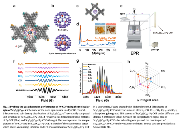
The electron spin sensor has high sensitivity and can be widely used to detect various physical and chemical properties, such as electric field, magnetic field, molecular or protein dynamics, nuclei or other particles, etc. These unique advantages and potential applications make spin-based sensors a hot research direction. Sc3C2@C80, with its highly stable electron spin protected by a carbon cage, is suitable for gas adsorption detection inside porous materials. Py-COF is a recently emerged porous organic framework material with unique adsorption properties. It is synthesized using self-condensation building blocks with formyl and amino groups, and its theoretical pore size is 1.38 nm. Therefore, a metallofullerene Sc3C2@C80 unit (with a size of approximately 0.8 nm) can enter a nanoscale pore of Py-COF.


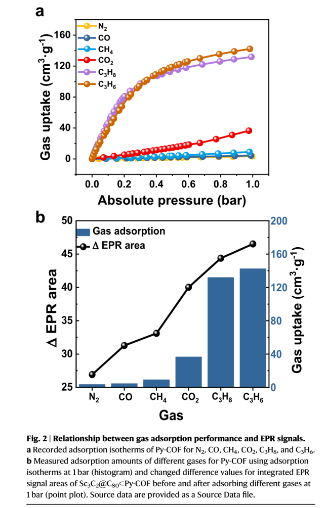
Researcher Wang from the Institute of Chemistry, Academy of Sciences, has developed a nano spin sensor based on metallofullerene for detecting gas adsorption inside porous organic frameworks. Paramagnetic metallofullerene, Sc3C2@C80, is embedded in nanoscale pores of a pyrene-based covalent organic framework (Py-COF). The EPR Spectroscopy (CIQTEK EPR200-Plus) is used to record the EPR signals of the embedded Sc3C2@C80 spin probe for N2, CO, CH4, CO2, C3H6, and C3H8 adsorbed within Py-COF. The study reveals that the EPR signals of embedded Sc3C2@C80 exhibit a regular dependence on the gas adsorption performance of Py-COF. The research findings are published in Nature Communications under the title "Embedded nano spin sensor for in situ probing of gas adsorption inside porous organic frameworks. "

 CIQTEK EPR Spectroscopy assists research on nano-spin sensors

Using Sc3C2@C80 as a molecular spin probe to investigate the gas adsorption performance of PyOF


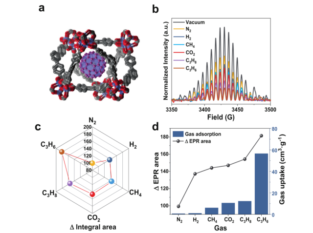
In the study, the authors used a paramagnetic metallofullerene, Sc3C2@C80 (size approximately 0.8 nm), as a spin probe embedded in a pyrene-based covalent organic framework (Py-COF) nanocage to detect gas adsorption in Py-COF. The adsorption performance of N2, CO, CH4, CO2, C3H6, and C3H8 gases in Py-COF was investigated by monitoring the embedded Sc3C2@C80 Electron Paramagnetic Resonance (EPR) signal. The study demonstrated that the EPR signal of Sc3C2@C80 was systematically related to the gas adsorption performance of Py-COF. Additionally, unlike traditional adsorption isotherm measurements, this implantable nanoscale spin sensor enabled real-time gas adsorption and desorption monitoring. The proposed nanoscale spin sensor was also utilized to investigate the gas adsorption performance of a metal-organic framework (MOF-177), showcasing its multifunctionality.


 CIQTEK EPR Spectroscopy assists research on nano-spin sensors

Relationship Between Gas Adsorption Performance and EPR Signal

 CIQTEK EPR Spectroscopy assists research on nano-spin sensors

The effect of gas pressure on EPR signals

 CIQTEK EPR Spectroscopy assists research on nano-spin sensors

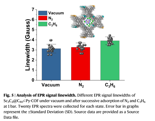
Analysis of EPR Signal LineWidth

 CIQTEK EPR Spectroscopy assists research on nano-spin sensors

Using the molecular spin method of Sc3C2@C80 to investigate the gas adsorption process in MOF-177

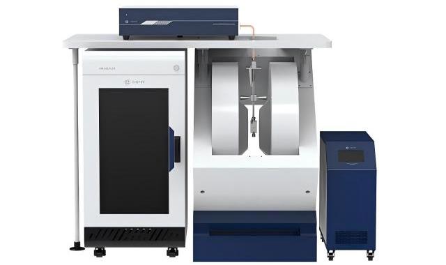
 X-Band CW-EPR Spectroscopy EPR200-Plus

X-Band CW-EPR Spectroscopy | EPR200-Plus


The CIQTEK EPR200-Plus Spectroscopy provides professional continuous wave Electron Paramagnetic Resonance solutions for industrial and academic users.


>> EPR200-Plus Accessories: Dual Mode Resonator, High-temperature System, Liquid Nitrogen Variable Temperature With Cryostat, Liquid helium Variable Temperature, Liquid Helium-free Dry Cryogenic System, Time-resolved EPR System, Goniometers, Irradiation system, Flat cell.


Electron paramagnetic resonance (EPR) or Electron Spin Resonance (ESR) spectroscopy is a powerful analytical method to study the structure, dynamics, and spatial distribution of unpaired electronics in paramagnetic substances. It can provide in-situ and non-destructive information on electron spins, orbitals, and nuclei at the microscopic scale. EPR spectroscopy is particularly useful for studying metal complexes or organic radicals so it has important applications in the fields of chemistry, materials, physics, environment, etc.


Infinity Mirror Signage have become a popular DIY project for those looking to add a touch of modern artistry and glamor to their home decor. With the mesmerizing illusion of infinite depth, infinity mirrors can transform any space into a captivating visual experience. Whether you're a seasoned DIYer or just getting started, making your own infinity mirror signage is a rewarding project that combines creativity with basic technical skills.


  • First Materials Needed:

Before you begin, gather the following materials:

Mirror: A standard mirror to serve as the base for the infinity mirror.

Bi-directional mirror film: This is essential for creating the illusion of depth. You can purchase pre-made two-way mirrors or you can apply film to the glass.

LED Light Strips: These will be used to create the illusion of endless light in the mirror. Choose a color that matches your aesthetic or opt for color-changing LED lights for a dynamic effect.

Wood or Metal Frame: The frame will hold the mirror and the double glazing. Make sure it is sturdy enough to withstand the weight.

LED Light Power Supply: Depending on the LED strip, you may need a specific power supply or adapter.

  • Step-by-step guide:

Prepare the mirror frame:

Begin by assembling or preparing the frame for the mirror and two-way glass. If you are using a wooden frame, cut it to the proper size and make sure the frame fits the mirror snugly. The frame should be deep enough to accommodate the thickness of the mirror and two-way glass as well as the LED lights.

Mounting the Mirror:

Attach the standard mirror to the back of the frame. This mirror will act as a base layer to reflect the light from the LED lamps.

Install the LED Lights:

Position the LED strips towards the mirror on the inside edge of the frame. Make sure the lights are evenly spaced for a uniform effect. Connect the lights to the power supply, but do not turn them on yet.

Install the two-way mirror:

If you are using a two-way mirror film, carefully apply it to the second piece of glass. Make sure there are no air bubbles or creases as these can ruin the illusion. If you are using a pre-made two-way mirror, simply place it on top of the frame with the reflective side facing the mirror.

Assemble the infinity mirror:

Place the two-way mirror on top of the frame and secure it in place. The two-way mirror should be positioned so that it reflects both the LED light and the standard mirror, creating the illusion of infinite light.

Activate and enjoy:

Once everything is in place, turn on the LED lights. The light will reflect between the two mirrors, creating the mesmerizing illusion of infinite depth. If your LED lights have the ability to adjust brightness and color settings, you can find the perfect look for your space.

Customization Tip:

Shapes and Sizes: Infinity mirrors aren't limited to traditional squares or rectangles. Consider using round or geometric frames for a more unique look.

LED Effects: Experiment with different LED effects such as fading, pulsing or color shifting to enhance visual appeal.

Mounting Options: Depending on size and design, Infinity mirrors can be mounted on a wall, framed as artwork, or even used as a tabletop display.


DIYing your own Infinity Mirror is not only a fun project, but also a way to personalize your space with a truly unique piece of art. Whether you're looking to enhance your home décor or create a conversation piece, infinity mirrors combine visual interest with modern elegance. With just a few basic materials and a little creativity, you can craft mesmerizing optical illusions that will make anyone swoon.

In The Pursuit Of Space Aesthetics And Practical Functions Today, Lighting Design Has Become An Indispensable Part Of Interior Decoration. With The Advancement Of Technology, Seenlamp Lighting Has Come Up With An Innovative Solution: Mini Embedded Downlights. These State-Of-The-Art Luminaires Offer Unique Features Including Mini Holes, Adjustable Design And Anti-Glare, Making Them Ideal For Commercial Applications Such As Museums, Art Galleries And Restaurants, As Well As Shopping Stores. The Following Is a Detailed Explanation Of The Advantages Of Mini Recessed Downlights For Seenlamp Lighting.

Adjustable Design

A Notable Feature Of The Mini Recessed Downlights Is Their Adjustable Design. These Lamps Have The Ability To Adjust The Light Direction Angle, Allowing The Flexibility To Direct The Light Exactly Where It Is Needed. This Versatility Allows For Targeted Lighting That Gives Emphasis To a Specific Artwork Or Merchandise In a Commercial Space. For Museums And Exhibition Halls, The Adjustable Design Of These Downlights Helps Create Sophisticated Lighting Effects That Highlight Exhibits And Emphasize Their Uniqueness. Similarly, In Stores, This Feature Ensures That Products Are Properly Displayed, Capturing The Attention Of Potential Customers And Enhancing The Overall Shopping Experience.

Energy Saving And Environmental Protectio

Mini Downlights Not Only Perform Well In Anti-Glare Eye Protection, But Also Have Significant Energy Saving And Environmental Protection Advantages. Led As Its Core Light Source, Has The Characteristics Of Low Energy Consumption, Less Heat, Compared With Traditional Lighting Products, Can Greatly Reduce Energy Consumption And Carbon Emissions. In Addition, The Led Light Source Also Has a Long Service Life, Reducing The Need For Frequent Replacement Of Lamps, Further Reducing The Cost Of Use And Environmental Burden.

Anti-Glare Eye Protection

The Mini Embedded Downlight Of Seenlamp Lighting Adopts The Structural Design Of Deep Buried Light Source And Can Add Honeycomb Network, So That It Effectively Avoids Direct Light Into People's Eyes, Reduces The Occurrence Of Blinding Phenomenon, So As To Protect People's Eyes. In Scenes That Require Partial Lighting, Such As Reading Areas, Work Areas Or Art Displays, Mini Recessed Downlights Provide Soft And Focused Light That Meets Lighting Needs While Protecting The User's Visual Health.

Very Integrated

The Compact Design And Small Size Of The Mini Recessed Downlights For Seenlamp Lighting Make Them Extremely Flexible During Installation. The Design Of Its Mini Opening And Extremely Narrow Frame Is Easier To Integrate Into The Ceiling And Integrate With The Ceiling To Create a More Refined And Advanced Sense Of Space. At The Same Time, Its Rich Color Choices Also Provide Users With More Personalized Choice Space, So That Lighting Becomes a Part Of The Space Decoration.

Conclusion

To Sum Up, Seenlamp's Mini Embedded Downlight Has Become a Bright Pearl In The Modern Lighting Market With Its Advantages Of Energy Saving, Environmental Protection, Small And Delicate, Anti-Glare Eye Protection, And Flexible Pendulum. It Not Only Brings Convenience And Comfort To Our Life, But Also Provides Strong Support For Our Pursuit Of a High-Quality Lifestyle.

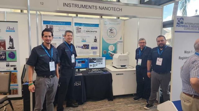
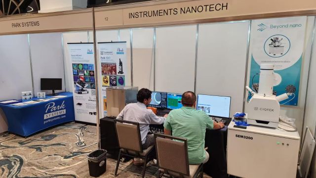
CIQTEK's Distributor Showcased  SEM3200 at the IMRC2024

IN, the distributor of CIQTEK, showcased the revolutionary SEM3200 at the 32nd International Materials Research Congress (IMRC2024scheduled for August 18-23), garnering attention from researchers and experts in the field.

CIQTEK's Distributor Showcased  SEM3200 at the IMRC2024

As an industry-leading Scanning Electron Microscope, the SEM3200 offers advanced imaging capabilities, enabling researchers to explore the intricacies of materials at the microscopic level.

CIQTEK's Distributor Showcased  SEM3200 at the IMRC2024

"We are excited to introduce the SEM3200 to the global research community at the IMRC2024. This instrument represents a significant advancement in scanning electron microscopy, providing researchers with powerful imaging capabilities and precise analytical tools." staff said, "We believe that the SEM3200 will revolutionize the way researchers examine and understand materials, contributing to advancements in various industries such as petrochemicals, environmental protection, biomedicine, and energy."


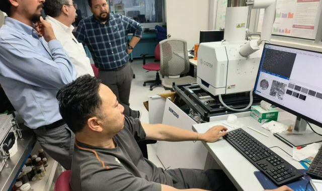
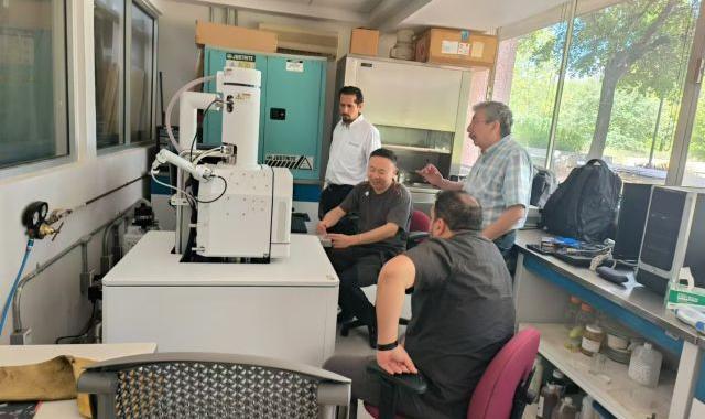
CIQTEK SEM3200 Installed Successfully in the Laboratory of the University of Monterrey, Mexico


CIQTEK has announced the successful installation of the SEM3200, a high-performance tungsten filament scanning electron microscope, at the prestigious Monterrey University laboratory. This advanced imaging system is set to revolutionize research in the field of characterize analysis and contribute to breakthroughs in various scientific disciplines.


CIQTEK SEM3200 Installed Successfully in the Laboratory of the University of Monterrey, Mexico


The principal investigator at the Monterrey University laboratory, expressed his excitement about the new SEM3200 installation, stating, "The addition of this cutting-edge scanning electron microscope will significantly advance our research capabilities. The high-resolution imaging and analytical features of the SEM3200 will allow us to gain invaluable insights into microscopic imaging and analysis. We anticipate this instrument will play a pivotal role in driving discoveries in our field."


CIQTEK SEM3200 Installed Successfully in the Laboratory of the University of Monterrey, Mexico


Electron paramagnetic resonance (EPR), or electron spin resonance (ESR), is a powerful spectroscopic technique used to study the properties of materials with unpaired electrons. To perform EPR experiments, it is crucial to prepare high-quality EPR samples. In this blog post, we will describe step-by-step how to prepare EPR samples.


>> Materials:

- Sample matrix: This can be a solid sample, solution, or powder.

- EPR Tube or Sample Holder: Choose the appropriate EPR tube or sample holder for your sample size.

- Sample Preparation Tools: Mortar and pestle (for grinding), weighing balance, spatula or pipette, and other materials associated with the sample.


>> Steps

Step 1: Selecting a Sample

Select an appropriate sample for the EPR study. It can be a pure compound, a mixture, or a biological sample containing paramagnetic species. Make sure that the sample contains unpaired electrons so that the EPR signal will show up.


Step 2: Sample Cleaning

If the sample is impure or contains contaminants, it must be purified to obtain reliable EPR data. Depending on the nature of the sample, use appropriate purification techniques such as recrystallization, extraction, or chromatography.


Step 3: Sample Preparation for Solid Samples

a) Grinding: If the sample is solid, grind it to a fine powder using a mortar and pestle. This helps to improve the homogeneity of the sample and ensures that the EPR signal is representative.


b) Weighing: Use an accurate weighing balance to weigh the appropriate amount of powdered sample. The amount required will vary depending on the EPR instrument and sample sensitivity.


c) Sample Loading: Carefully transfer the weighed sample into the EPR tube or sample holder. Ensure that the sample is evenly distributed within the tube to obtain accurate measurements.


Step 4: Sample Preparation for Solution Samples

a) Solvent Selection: Select a suitable solvent that will dissolve the sample and meet the requirements of the EPR experiment. Common solvents include water, ethanol, chloroform, or dimethyl sulfoxide (DMSO).


b) Concentration Determination: The concentration of paramagnetic material in solution is measured using established techniques such as UV-Vis spectroscopy or through a known calibration curve.


c) Sample Loading: Pipette the appropriate volume of solution into an EPR tube or sample holder. Take care to avoid air bubbles, which can affect the EPR signal and introduce artifacts.


Step 5: Sample Storage and Handling

Once the EPR samples have been prepared, store them under the appropriate conditions for the stability of the samples and the requirements of the experiment. Protect the sample from light, moisture, and temperature fluctuations to maintain its integrity.


>> Conclusion:

Preparation of EPR samples is a critical step for successful EPR experiments. Whether grinding and weighing a solid sample or preparing a solution, careful attention to detail and sample integrity are critical. Well-prepared samples ensure accurate and reliable EPR measurements and allow researchers to explore the fascinating world of electron parametric resonance.

It is also important to familiarize yourself with the specific instructions and guidelines provided by the EPR instrument manufacturer. CIQTEK EPR spectrometers offer comprehensive and detailed EPR sample configuration tutorials and a well-established team of dedicated professionals to answer questions and are fully committed to solving user challenges, anytime, for any issue.

Scanning Electron Microscopy (SEM) is a microscopy technique that uses a focused electron beam to create detailed images of the surface of a sample. The electron beam scans the sample in a raster pattern, and the resulting signals generated by interactions between the electron beam and the sample's surface are detected and used to form an image. SEM provides high-resolution three-dimensional surface images and is widely used in various fields, including material characterization, nanotechnology, and biological research.


Energy-Dispersive X-ray Spectroscopy (EDS): EDS is an analytical technique often used with SEM. It detects characteristic X-rays emitted by a sample when it is bombarded with an electron beam. The energy and intensity of these X-rays provide information about the elemental composition of the sample. SEM EDS allows the identification and quantification of elements present in the sample, offering valuable insights into its elemental makeup and chemical characterization.


Energy-Dispersive X-ray Analysis (EDX): EDX is another term for EDS and refers to the analysis and investigation of samples using energy-dispersive X-ray spectroscopy. It involves the detection and analysis of X-rays emitted from a sample, which carries information about the elements present and their concentrations. SEM EDX is a powerful tool for qualitative and quantitative elemental analysis, identifying trace elements, and mapping elemental distribution across a sample.


The combination of SEM and EDS/EDX offers several advantages and applications:


1. Elemental Analysis

SEM EDS/EDX allows for qualitative and quantitative elemental analysis of samples. It can identify the chemical composition and elemental distribution within a material, including trace elements.


2. Material Characterization

This technique is widely used for characterizing various materials, such as metals, minerals, polymers, ceramics, and biological samples. It helps determine the elemental composition, the presence of impurities, and the identification of phases or compounds within a sample.


3. Failure Analysis

SEM EDS/EDX is valuable in investigating material-related failures and defects. It can identify the causes of failures by analyzing the elemental composition and identifying foreign particles or contaminants.


4. Geological Analysis

SEM EDS/EDX is extensively utilized in geology to study the composition and structure of rocks, minerals, and soil. It aids in the identification of minerals, the study of rock textures, and the analysis of geological processes.


5. Forensic Science

SEM EDS/EDX plays a crucial role in forensic investigations, assisting in the analysis of trace evidence, such as fibers, gunshot residue, paint chips, and glass fragments. It can help identify and compare materials found at a crime scene.


Overall, EDS/EDX in SEM is a powerful analytical tool that combines imaging and elemental analysis. It finds applications in various fields, including materials science, geology, forensic science, environmental analysis, biology, and archaeology.


CIQTEK's self-developed SEM Microscopes offer a wide range of electron detectors, such as BSED, STEM, EDS, EDX, EBSD, In-lens, ETD, etc. 


Scanning Electron Microscope