Exploring Types of Scanning Electron Microscopes
Microscopy has revolutionized our understanding of the microscopic world, enabling scientists to reveal complex structures and study materials at the nanoscale. Among the various powerful microscopes, the scanning electron microscope (SEM) is an indispensable tool for imaging surfaces with extraordinary detail and resolution.
In this blog post, we will look in-depth at different types of scanning electron microscopes and explore their unique capabilities and applications.
Conventional Scanning Electron Microscope (C-SEM)
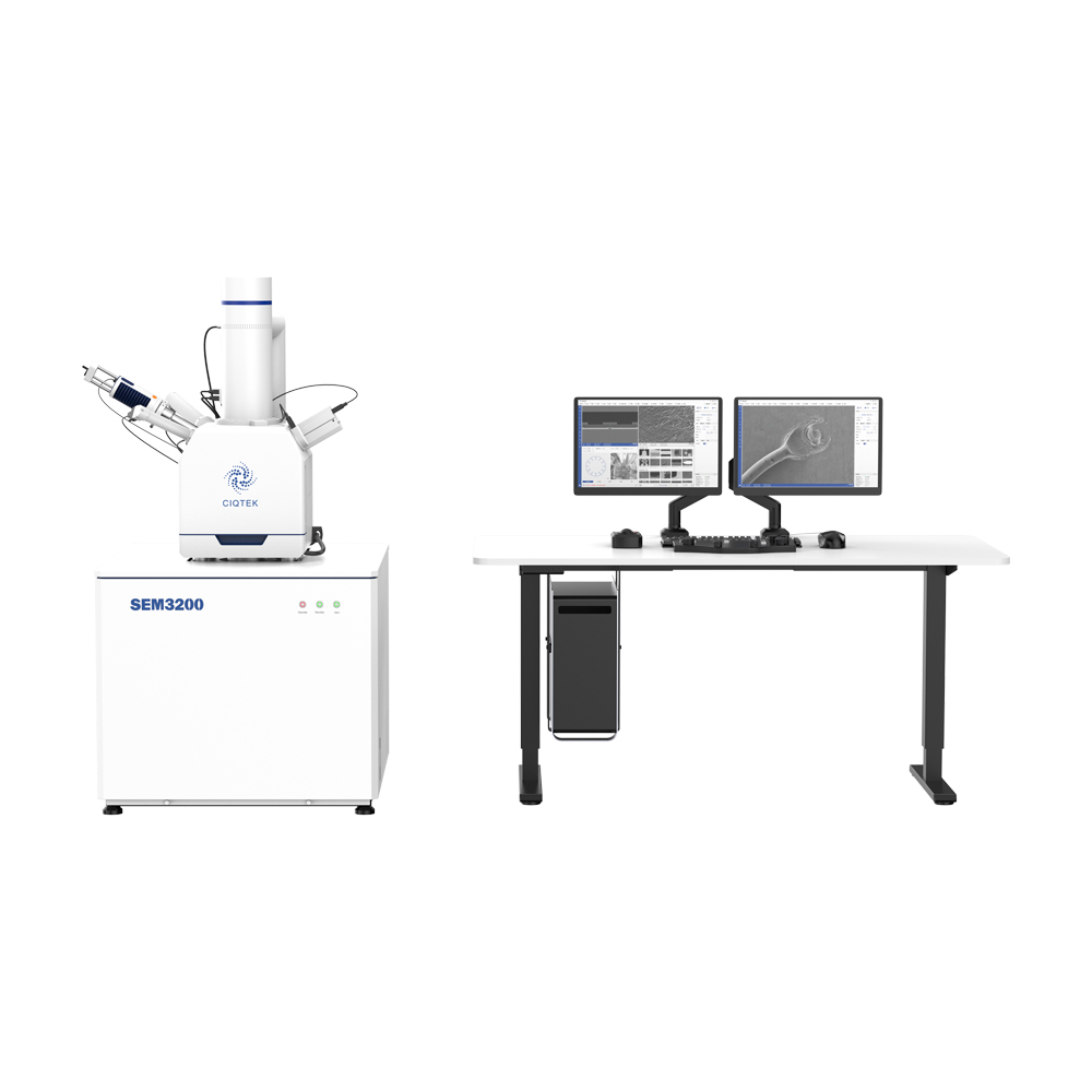
A conventional scanning electron microscope, also known as a single-beam scanning electron microscope, is the most common type. It consists of an electron source that generates a high-energy electron beam, which is focused and scanned over the surface of a specimen. An electron detector captures the resulting signal and constructs a high-resolution image. The C-SEM is a versatile instrument capable of imaging a wide range of samples, including biological samples, materials, and semiconductor devices.
 Check CIQTEK C-SEM Tungsten Filament SEM - SEM3200
Environmental Scanning Electron Microscope (ESEM)
Designed to analyze samples in their natural or hydrated state, environmental scanning electron microscopes are therefore suitable for studying fragile or aqueous samples. Unlike C-SEM, ESEM can image under different pressure conditions without the need for extensive sample preparation. This type of scanning electron microscope is particularly suitable for life sciences, geology, and environmental studies.
Field Emission Scanning Electron Microscope (FE-SEM)
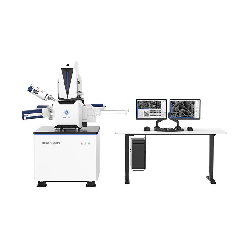
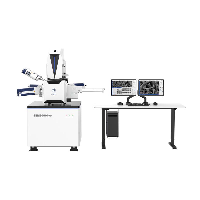
Field Emission Scanning Electron Microscopes utilize field emitters as an electron source to produce electron beams of incredible intensity, resulting in improved resolution and signal detection. With atomic-level resolution, FE-SEMs are ideal for examining advanced materials, analyzing nanoparticles, and studying nanoscale structures. They have applications in materials science, nanotechnology, and semiconductor research.
Check CIQTEK Ultra-high Resolution FESEM - SEM5000X
Low-Voltage Scanning Electron Microscopy (LV-SEM)
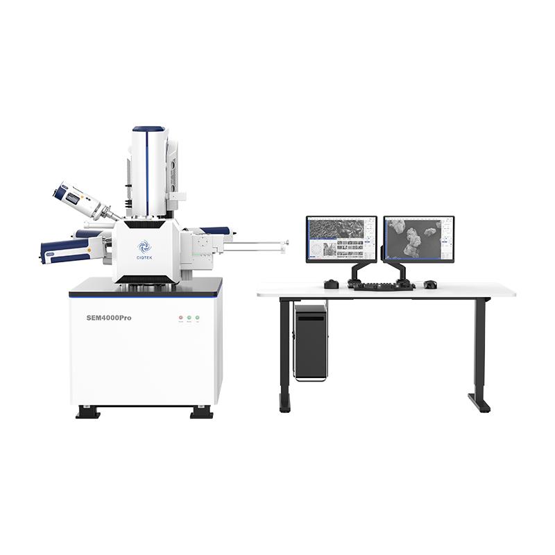
LV-SEMs operate at relatively low voltages compared to C-SEMs, which provides a distinct advantage for imaging non-conductive or beam-sensitive materials. By operating at lower voltages, LV-SEM minimizes damage to the sample and enhances imaging of insulated samples without the need for conductive coatings.LV-SEM can be applied to biological research, polymers, and poorly conductive materials.
Variable Pressure Scanning Electron Microscopy (VP-SEM)
Variable Pressure Scanning Electron Microscopy combines the capabilities of a conventional scanning electron microscope and an ambient scanning electron microscope to image samples that have limited vacuum compatibility or are susceptible to surface charging. By introducing gas into the scanning electron microscope chamber, VP-SEMs mitigate charging effects and provide high-resolution imaging of non-conductive materials. This makes them suitable for applications in forensic science, archaeology, and art conservation.
Scanning electron microscopes have become indispensable tools for researchers in a variety of fields. From the versatile C-SEM to the specialized FE-SEM, ESEM, LV-SEM, and VP-SEM, various types of scanning electron microscopes offer powerful imaging capabilities based on different sample characteristics and requirements. These state-of-the-art instruments continue to drive scientific discovery, pushing the boundaries of our understanding of the nanoworld and opening up new areas of research in different fields.


