Application Cases | Low Voltage, High Resolution! Application of SEM5000X in Molecular Sieve Research
Molecular sieves are artificially synthesized hydrated aluminosilicates or natural zeolites with molecular sieving properties. They have uniformly sized pores and well-arranged channels and cavities in their structure. Molecular sieves of different pore sizes can separate molecules of different sizes and shapes. They possess functions such as adsorption, catalysis, and ion exchange, which give them tremendous potential applications in various fields such as petrochemical engineering, environmental protection, biomedical, and energy.
In 1925, the molecular separation effect of zeolite was first reported, and zeolite acquired a new name — molecular sieve. However, the small pore size of zeolite molecular sieves limited their application range, so researchers turned their attention to the development of mesoporous materials with larger pore sizes. Mesoporous materials (a class of porous materials with pore sizes ranging from 2 to 50 nm) have extremely high surface area, regularly ordered pore structures, and continuously adjustable pore sizes. Since their inception, mesoporous materials have become one of the interdisciplinary frontiers.
For molecular sieves, particle size and particle size distribution are important physical parameters that directly affect product process performance and utility, particularly in catalyst research. The crystal grain size, pore structure, and preparation conditions of molecular sieves have significant effects on catalyst performance. Therefore, exploring changes in molecular sieve crystal morphology, precise control of their shape, and regulating and enhancing catalytic performance are of great significance and have always been important aspects of molecular sieve research. Scanning electron microscopy provides important microscopic information for studying the structure-performance relationship of molecular sieves, aiding in guiding the synthesis optimization and performance control of molecular sieves.
ZSM-5 molecular sieve has an MFI structure. The product selectivity, reactivity and stability of MFI-type molecular sieve catalysts with different crystal morphologies may vary depending on the morphology.
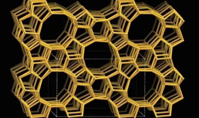
Figure 1(a) MFI skeleton topology
The following are images of ZSM-5 molecular sieve captured using the CIQTEK High-Resolution Field Emission Scanning Electron Microscope SEM5000X.
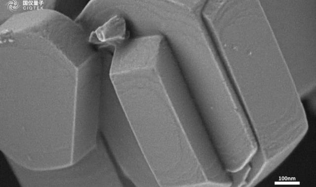
Figure 1(b) ZSM-5 molecular sieve/500V/Inlens
SBA-15 is a common silicon-based mesoporous material with a two-dimensional hexagonal pore structure, with pore sizes typically ranging from 3 to 10 nm. Most mesoporous materials are non-conductive, and the commonly used pre-treatment method of coating (with Pt or Au) may block the nanoscale pores, affecting the characterization of their microstructure.
Therefore, such samples are usually not subjected to any coating pre-treatment, which requires the scanning electron microscope to have ultra-high resolution imaging capability even at extremely low voltages.
The following are images of SBA-15 molecular sieve captured using the CIQTEK High-Resolution Field Emission Scanning Electron Microscope SEM5000X.
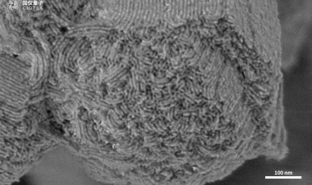
Figure 2 SBA-15/500V/Inlens
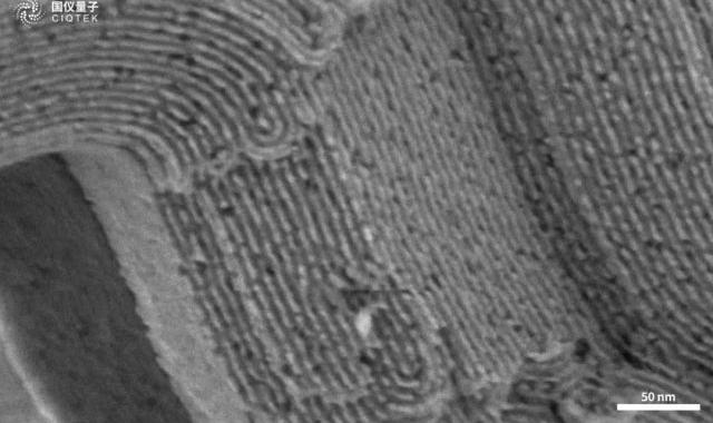
SBA-15/500V/Inlens
The SEM5000X is a high-resolution field emission scanning electron microscope with a breakthrough resolution of 0.6 nm @ 15 kV and 1.0 nm @ 1 kV.
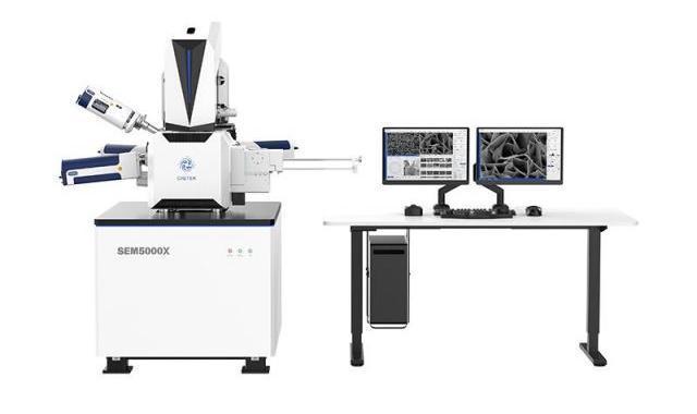
Equipped with an in-column deceleration technology, the SEM5000X supports an optional sample stage deceleration mode to further reduce lens aberration and improve image resolution at low voltages.
The term "deceleration" refers to applying negative pressure on the sample stage to decelerate the high-energy electron beam before it reaches the sample surface. In the deceleration mode, it maintains brightness, signal-to-noise ratio, and high resolution under high accelerating voltage, while effectively reducing sample charging at low landing voltage. Additionally, under the influence of the deceleration electric field, the signal electrons are accelerated, improving the detection efficiency of the corresponding detectors and increasing the signal-to-noise ratio of low voltage images
