Demand for silicon wafers soars
Recently, there has been a lot of discussion about silicon wafers. Here we analyze it from several perspectives:

First of all, in terms of demand, thanks to the rise of new applications such as 5G, artificial intelligence (AI), and electric vehicles, the demand for semiconductors has increased significantly, and the shortage of chips and the expansion of foundry production have continued to benefit, and the industry market is hot. According to the statistics of the International Semiconductor Industry Association (SEMI), the global semiconductor silicon wafer shipment area will continue to grow until 2024, and show a new high performance year by year.
The huge increase in demand for silicon wafers is related to the large-scale expansion of global wafer factories in recent years. According to SEMI statistics, the number of global semiconductor factories in 2019 was 957, and it is expected to grow to 1,011 in 2022. The monthly production capacity of the factory often jumps from 30,000 to 50,000 pieces. Silicon wafers have become an indispensable strategic material, and their usage will inevitably rise in a straight line.
On the other hand, assessed from the supply side, SEMI expects global silicon wafer shipments to hit a record high year by year in the next three years. Silicon wafer manufacturers at home and abroad are unanimously optimistic about the market. After all, the foundry capacity is full, and it is undoubtedly the strongest and powerful backing for the silicon wafer industry, which is the most critical upstream raw material.
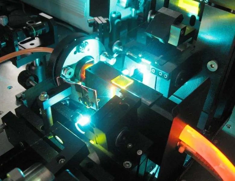
The Optical Fiber Bundles and Light Sources produced by Hecho Technology are widely used in the semiconductor industry, such as wafer inspection, cutting, Laser Direct Imaging, Automatic Optical Inspection and other fields. Different needs of different customers.