The field of Scanning Electron Microscopy (SEM) continues to advance rapidly, driving innovation across materials science, life sciences, and nanotechnology. Attending conferences and exhibitions provides invaluable opportunities for professionals and researchers in this domain to learn about cutting-edge technologies, share research, and network with peers. Below is a list of some of the important SEM events in the United States for 2025.


1. Microscopy & Microanalysis (M&M) 2025

  • Dates: July 27 – July 31, 2025

  • Location: Salt Lake City, Utah

The Microscopy & Microanalysis (M&M) conference is one of the premier events for electron microscopy professionals. Organized by the Microscopy Society of America (MSA) and the Microanalysis Society (MAS), this conference covers all aspects of microscopy and microanalysis. Expect various technical sessions, hands-on workshops, and an extensive exhibition featuring the latest SEM technologies.
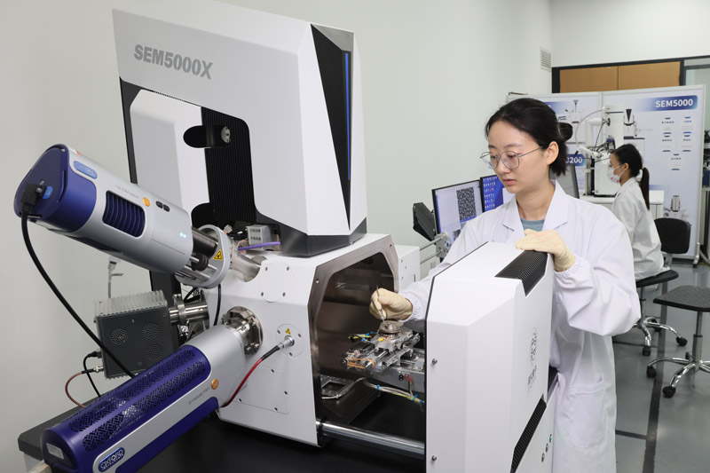
 

CIQTEK SEM Microscope  CIQTEK SEM will attend the M&M2025 as always. Visit at booth #1303.


2. Materials Research Society (MRS) Spring and Fall Meetings

  • Spring Meeting & Exhibit: April 7–11, 2025 | Seattle, Washington

  • Fall Meeting & Exhibit: November 30–December 5, 2025 | Boston, Massachusetts

Both the Spring and Fall MRS Meetings are essential gatherings for materials scientists. These events feature sessions on advanced characterization techniques, including SEM. Researchers can present their findings, attend specialized symposia, and explore exhibits showcasing state-of-the-art microscopy tools.


3. Pittcon 2025

  • Dates: March 1–5, 2025

  • Location: Boston, Massachusetts

Pittcon is a leading conference and expo on laboratory science. While it spans a wide range of analytical techniques, the event often features sessions and exhibitors dedicated to SEM and its applications in chemical analysis and materials characterization.
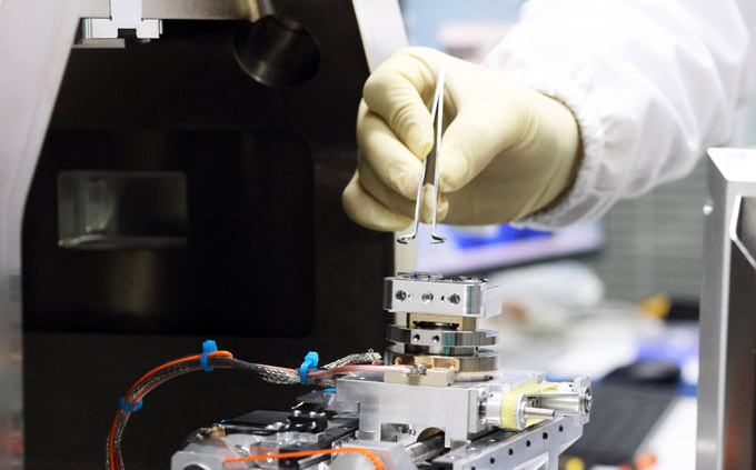
 

CIQTEK SEM Microscope  CIQTEK SEM will attend the Pittcon 2025. Visit at booth #625.


Why Attend SEM Microscope Meetings?

  • Stay Updated: Learn about the latest SEM microscope technologies, methodologies, and applications.

  • Network: Connect with leading researchers, industry professionals, and equipment manufacturers.

  • Collaborate: Explore opportunities for partnerships and collaborative research.

  • Professional Development: Participate in workshops and training sessions to enhance your skills.

Attending these conferences can provide a significant boost to your professional knowledge and network, ensuring you stay at the forefront of SEM advancements. Mark your calendar and plan to attend these pivotal events in 2025!
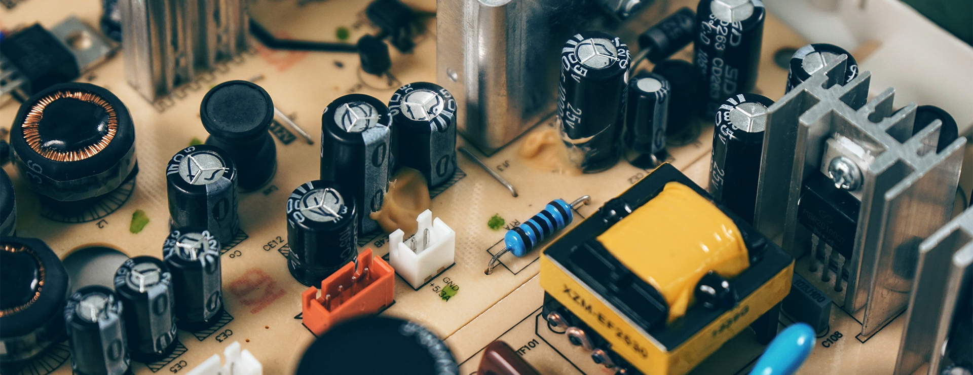
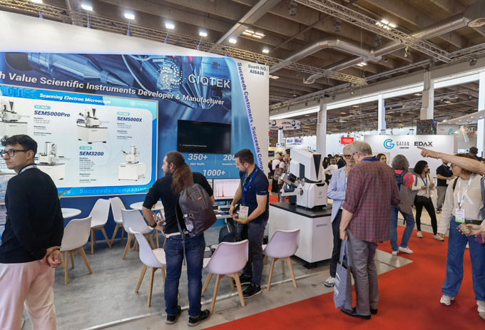
CIQTEK SEM Microscope at Exhibition


Hey everyone! I'm excited to introduce you to the new North Edge LONG WINGS solar watch that I just got, and it's absolutely amazing!

We don't have to worry about changing batteries anymore, and it charges quickly even in low light. The 180-day full charge battery life is incredible. I can go on long hikes, camping trips, or even just forget to take it off for a while, and it still keeps ticking.

The time veracity of 30 sec/month is really accurate. I'm always on time for my meetings and appointments. The triple chronograph is so handy for timing my workouts at the gym or when I'm cycling outdoors. It helps me track my progress and improve my performance.

The clear at night display is really cool. I can easily see the time when I wake up in the middle of the night without having to turn on the light and disturb my sleep. The 50M waterproof rating is great for when I go swimming or if I get caught in the rain. The tri-fold clasp with push button switch is very convenient and makes it easy to put on and take off.

And let's not forget about the 316 stainless steel construction. It looks so sleek and stylish, and I know it's going to last a long time. The brand LOGO on the bezel case and the strap just adds to the overall cool factor. 

I highly recommend the North Edge LONG WINGS to anyone who wants a great watch that can keep up with their active lifestyle.


     Hey everyone! Today, I'm super excited to share my thoughts on the Smart Watch QX7 Pro.
 
North edge watch supplier
First off, the 2.0 - inch HD retina display is a stunner. With a resolution of 240*282 pixels, every icon, every notification, looks sharp and vibrant. Whether I'm checking my messages or tracking my workout stats, the visual experience is top - notch.
 
The health - monitoring features are a huge plus. Knowing my heart rate and blood pressure throughout the day gives me peace of mind. And the real - time temperature monitoring? It's a nifty addition, especially during flu seasons.
 
In terms of sports, the 100 + sport modes have been a game - changer. Whether I'm hitting the gym for a weightlifting session or going for a run, the watch accurately tracks my progress. And let's not forget the high - fidelity speaker. Listening to music during my workouts has never been clearer.

-----------------------------

Overall, the Smart Watch QX7 Pro has seamlessly integrated into my daily life, making it more organized, healthier, and more enjoyable. 


Scanning electron microscopes (SEMs) are essential for modern research and industrial applications, allowing detailed imaging and analysis of nanoscale materials. However, investing in a scanning electron microscope is a big decision, and understanding its pricing structure is crucial for potential buyers. In this blog, we will analyze the factors that affect the cost of an SEM, typical price ranges, and additional costs to consider.


What affects the cost of an SEM?

The price of an SEM varies greatly depending on its specifications, features, and intended application. Here are some key factors:

1. Resolution and Performance

High-resolution SEMs capable of imaging at the nanometer or sub-nanometer level are typically more expensive. Advanced models have enhanced imaging capabilities such as higher magnification and better signal-to-noise ratios.


2. Additional Features

Modern SEMs usually have the following additional features:

- Energy dispersive X-ray spectroscopy (EDS) for elemental analysis.

- Electron Backscatter Diffraction (EBSD) for crystallographic studies.

- Environmental SEM (ESEM) is used to image wet or biological samples.

Each of these capabilities adds to the total cost.


3. Automation and Software

SEMs with automation features such as autofocus, auto diffuser, and advanced image processing software are more expensive. These features improve ease of use and productivity, especially in high-throughput environments.


4. Brands and Manufacturers

Leading manufacturers such as Thermo Fisher Scientific, Zeiss, JEOL, and CIQTEK typically offer a range of models, with premium models at a higher price point. CIQTEK, in particular, has a reputation for providing high-quality SEM solutions that combine performance and affordability, making it a cost-effective choice for many laboratories.

CIQTEK SEM Microscopes


5. Size and portability

Benchtop or desktop SEMs are more affordable and compact, making them suitable for small labs or educational purposes. On the other hand, full-size SEMs offer higher performance but are expensive.


Typical Price Ranges for Scanning Electron Microscopes

> Entry-level scanning electron microscopes: $50,000 - $100,000

These models are designed for basic imaging and are popular in educational institutions and small laboratories.

> Mid-range SEM: $100,000 - $300,000

Mid-range SEMs are ideal for research labs and industrial applications, with higher resolution and additional features such as EDS.

> High-end SEM: $300,000 - $1,000,000+

These systems are equipped with cutting-edge technology for advanced research and applications such as nanotechnology and semiconductor manufacturing.


Other Costs to Consider

When budgeting for SEM, it is important to consider the associated costs:

1. Installation and Training

Installation fees and operator training add to the initial cost. Manufacturers often include these services in the purchase package or charge an additional fee for them.

2. Maintenance and Service Contracts

Regular maintenance is essential for optimal SEM performance. Service contracts can range from $5,000 to $20,000 per year depending on the system's complexity.

3. Consumables and Accessories

- Conductive coatings for non-conductive samples.

- Sample holders and stubs.

- Replacement parts such as filaments or detectors.

4. Laboratory Infrastructure

High-performance scanning electron microscopes may require specific environmental conditions such as vibration isolation, temperature control, and specialized power supplies, which can increase setup costs.


Conclusion

Scanning electron microscopes can cost anywhere from a few tens of thousands of dollars to over a million dollars, depending on the model and features. While the initial price is an important consideration, potential buyers should also take into account long-term costs such as maintenance, consumables, and lab infrastructure. Knowing these factors will allow you to make an informed decision based on your research or industrial needs.

If you are considering investing in an SEM, consult with the manufacturer to discuss your specific requirements and receive a tailored quote. With the right system, an SEM can be a transformative addition to your analytical capabilities.

Crystal frequency stability refers to a crystal oscillator's ability to maintain a consistent frequency over time under varying conditions. This stability is essential in applications such as wireless communication, GPS systems, and precision instrumentation, where even minor deviations can lead to significant errors.

Stability is typically assessed over three primary domains:

Short-term stability, influenced by noise and phase fluctuations.

Medium-term stability, impacted by environmental factors like temperature and humidity.

Long-term stability, subject to aging and material degradation.

                                   How to improve crystal frequency stability 

Key Factors Affecting Crystal Oscillator Frequency Stability

Understanding the variables that affect stability is crucial for selecting and designing reliable crystal oscillators. Below are some of the most influential factors:

1. Temperature Variations

Temperature changes significantly impact the frequency of quartz crystals. A well-designed oscillator compensates for these effects through temperature-compensated crystal oscillators (TCXO) or oven-controlled crystal oscillators (OCXO). Advanced applications often require TCXOs or OCXOs to minimize low temperature drift in crystal frequency, ensuring consistent performance in extreme environments.

2. Load Capacitance

The external load capacitance in the circuit affects the resonant frequency of the crystal oscillator. Variations in load capacitance lead to deviations in the output frequency. Designers must carefully select and stabilize the load capacitance to reduce its impact, especially in precision systems where frequency stability is paramount.

3. Mechanical Vibrations and Stress

Physical stress or vibrations can induce minor deformations in the crystal structure, leading to shifts in frequency. Proper mounting techniques and vibration-resistant designs can mitigate these effects.

4. Aging

Crystals naturally degrade over time due to molecular changes and contamination. This process, known as aging, causes a slow but steady drift in frequency. Selecting high-quality crystals with low aging rates is essential for long-term stability.

Applications Requiring High Stability Crystal Oscillators

High-stability oscillators are indispensable in various fields where precision and reliability are crucial. Some prominent applications include:

· Telecommunications: Base stations and network equipment rely on highly stable oscillators to maintain synchronization across systems.

· Navigation Systems: GPS and aviation navigation demand exceptional frequency stability to provide accurate positioning data.

· Medical Devices: Equipment such as ultrasound machines and ECG monitors depend on stable frequencies to ensure reliable operation.

· IoT Devices: Low-power and long-range IoT applications benefit from stable oscillators to maintain consistent connectivity.

                                            How to improve crystal frequency stability 

The growing demand for precision across industries has driven advancements in oscillator technology, further enhancing their stability and adaptability.

How to Improve Crystal Frequency Stability

Achieving better frequency stability requires a combination of careful component selection, optimized circuit design, and external compensation techniques. Here are some strategies:

1. Temperature Compensation

Using TCXOs or OCXOs is one of the most effective methods to address temperature-related drift. These oscillators include mechanisms to counteract temperature variations, maintaining a stable output frequency.

2. Circuit Optimization

Minimizing noise in the oscillator circuit helps improve short-term stability. Ensuring a stable power supply and shielding the oscillator from electromagnetic interference can also enhance overall performance.

3. Proper Load Capacitance Matching

Accurate matching and stabilization of the load capacitance are vital for reducing its impact on the oscillator's frequency. This step is especially important in applications where frequency precision is non-negotiable.

4. High-Quality Crystals

Selecting crystals with low aging rates and high Q-factor improves long-term and medium-term stability. Manufacturers often specify the stability characteristics of crystals, enabling designers to choose the best match for their requirements.

The Future of Frequency Stability

With advancements in material science and manufacturing techniques, crystal oscillators are becoming increasingly robust. MEMS oscillators, while still in development for certain high-precision applications, offer alternative solutions with comparable frequency stability and additional benefits like compact size and resistance to mechanical stress.

In the context of high stability crystal oscillator applications, the demand for ultra-reliable components is likely to grow with the expansion of technologies such as 5G networks, autonomous vehicles, and space exploration.

Crystal frequency stability plays a pivotal role in the operation of modern electronic systems, influencing their accuracy and dependability. Factors like temperature variations, load capacitance, and aging must be carefully managed to ensure optimal performance. By leveraging high-quality crystals and advanced compensation techniques, designers can achieve the stability required for demanding applications.

The journey to perfect frequency stability is ongoing, but with continued innovation, crystal oscillators will remain at the heart of precision electronics, shaping the future of technology.Shenzhen Jingguanghua Electronics Co., Ltd. specializes in providing crystal oscillators, the most scientific solutions in various circuit applications. If you have any demand for crystal oscillator products, please contact us.

Crystal oscillators are a fundamental component in modern electronic circuits, widely used in devices such as computers, smartphones, and communication systems. They are essential for generating precise clock signals that synchronize the operation of electronic components. Among crystal oscillators, two main types are commonly discussed: active crystal oscillators and passive crystal oscillators.

What Are Active and Passive Crystal Oscillators?


Active Crystal Oscillators

Active crystal oscillators are self-contained modules that include a crystal resonator and an internal oscillation circuit. These oscillators generate clock signals directly without requiring additional external components. The internal circuit usually comprises an amplifier and feedback network, which help sustain the oscillations initiated by the crystal.

Key features of active crystal oscillators:

· They are pre-configured and ready to use.

· They generate output signals with a specific frequency determined by the crystal inside.

· They typically operate at higher frequencies compared to passive oscillators.

Passive Crystal Oscillators

Passive crystal oscillators, also referred to as crystal resonators, are simpler components that consist only of a quartz crystal. Unlike active oscillators, passive ones require an external circuit (e.g., a microcontroller or discrete components like resistors, capacitors, and amplifiers) to function. The external circuit excites the crystal to produce oscillations.

Key features of passive crystal oscillators:

· They rely on external components to generate oscillations.

· They are more basic and compact in design.

· They are typically used in lower-frequency applications.

  Working Principles of Active and Passive Crystal Oscillators


Active Oscillator Working Principle

Active oscillators function as integrated modules where the quartz crystal and oscillation circuit work together to generate a stable frequency. The crystal acts as a frequency-determining element, while the internal feedback amplifier sustains oscillations. The output signal from an active oscillator is a clean, high-frequency waveform, often used directly in digital systems.

Passive Oscillator Working Principle

Passive oscillators operate by exploiting the piezoelectric property of quartz crystals. When an external AC voltage is applied across the crystal, it vibrates at its natural resonant frequency. The resonant frequency is determined by the crystal's physical dimensions and cut. The oscillation signal is then amplified and conditioned by external circuitry to achieve the desired waveform and amplitude.

Differences Between Active and Passive Crystal Oscillators

Feature

Active Crystal Oscillator

Passive Crystal Oscillator

Components

Contains an internal oscillation circuit

Only includes a quartz crystal

External Circuitry

No additional components needed

Requires external circuit for oscillation

Output Signal

Generates ready-to-use output

Output depends on external circuit

Frequency Range

Operates at higher frequencies

Typically used for lower frequencies

Power Consumption

Consumes more power due to internal circuit

Lower power consumption overall

Size

Larger due to integrated circuit

Smaller and more compact

Ease of Use

Plug-and-play; no design complexity

Requires expertise in circuit design

Cost

Generally more expensive

More cost-effective


Applications of Active and Passive Crystal Oscillators


Applications of Active Crystal Oscillators

Active crystal oscillators are used in applications where high precision, reliability, and ease of integration are essential. Common applications include:

· Microprocessors and Microcontrollers: Used to provide accurate clock signals for timing and synchronization.

· Communication Systems: Ensure stable carrier frequencies for transmitters and receivers.

· Industrial Automation: Provide clock sources for PLCs and sensors.

· High-Speed Interfaces: Used in Ethernet, USB, and other high-speed data transfer protocols.

                          Applications of Active Crystal Oscillators

Applications of Passive Crystal Oscillators

Passive crystal oscillators are commonly found in simpler, cost-sensitive applications. Examples include:

· Low-Cost Microcontrollers: Used in devices like home appliances and remote controls.

· Consumer Electronics: Found in products such as digital clocks, wristwatches, and calculators.

· Frequency Filters: Used in circuits requiring frequency selection or filtering.

· Embedded Systems: Often paired with external components to create a customized oscillation circuit.

                                                    Applications of Passive Crystal Oscillators


Advantages and Disadvantages


Advantages of Active Crystal Oscillators

1. Ease of Integration: No need for external components, simplifying circuit design.

2. High Precision: Provide stable and accurate frequency signals.

3. Wide Frequency Range: Suitable for high-frequency applications.

4. Reduced Design Complexity: Ideal for engineers working on time-sensitive projects.

Disadvantages of Active Crystal Oscillators

1. Higher Cost: More expensive due to the integrated circuit.

2. Larger Size: Takes up more PCB space compared to passive oscillators.

3. Higher Power Consumption: Unsuitable for battery-powered or low-power applications.

Advantages of Passive Crystal Oscillators

1. Cost-Effective: Affordable for budget-sensitive designs.

2. Compact Size: Ideal for space-constrained applications.

3. Low Power Consumption: Well-suited for energy-efficient designs.

Disadvantages of Passive Crystal Oscillators

1. Requires External Components: Increases design complexity.

2. Limited Frequency Range: Typically supports lower frequencies.

3. Dependence on Circuit Design: Performance is highly dependent on the quality of the external circuit.

Factors to Consider When Choosing Between Active and Passive Crystal Oscillators

When deciding which type of crystal oscillator to use, consider the following factors:

· Frequency Requirements: Active oscillators are better for high-frequency applications.

· Power Constraints: Passive oscillators are preferred for low-power designs.

· Cost Considerations: Passive oscillators are more budget-friendly, while active ones may justify their higher cost in performance-critical applications.

· Space Limitations: Choose passive oscillators for compact designs.

· Ease of Design: Opt for active oscillators if you want a plug-and-play solution.

Active and passive crystal oscillators serve distinct purposes in electronic systems, each offering unique advantages and trade-offs. Active oscillators provide convenience and precision, making them suitable for high-performance applications, while passive oscillators are cost-effective and energy-efficient, ideal for simpler systems. By understanding their differences in components, working principles, and applications, you can make an informed decision for your specific project needs.

Whether designing a high-speed communication system or a low-cost consumer device, selecting the right type of crystal oscillator is crucial for ensuring optimal performance and reliability.


What Are the Electrical Properties and Dimensional Stability of TLX-8 PCB?


Introduction

The TLX-8 PCB 30mil is a highly versatile and reliable high volume antenna material designed to offer exceptional performance in a wide range of RF applications.

This PTFE fiberglass laminate material boasts a host of impressive features, including excellent PIM values, outstanding mechanical and thermal properties, low and stable Dk (Dielectric Constant), and dimensional stability. Its resistance to extreme environments, radiation, high temperatures, and moisture absorption make it suitable for demanding applications such as space launch, engine modules, warship antennas, and altimeter substrates.


This blogarticle will delve into the various benefits, properties, construction details, and typical applications of the Taconic TLX-8 PCB, highlighting why it is an excellent choice for radar systems, mobile communications, microwave test equipment, microwave transmission devices, amplifiers, and more.


 Taconic TLX-8 PCB 


Benefits

The TLX-8 30mil Taconic PCB Substrate offers a plethora of advantages that make it a suitable choice for demanding RF applications:


1) Excellent PIM Values:

With PIM values measured lower than -160 dBc, it ensures exceptional signal integrity and minimized interference.


2) Superior Mechanical & Thermal Properties:

The material provides robust mechanical reinforcement and exhibits excellent thermal stability, making it suitable for harsh environments.


3) Low and Stable Dk:

The TLX-8 High Frequency PCB maintains a low and stable Dielectric Constant, ensuring predictable electrical performance throughout a wide range of frequencies.


4) Dimensional Stability:

It demonstrates exceptional dimensional stability, preventing warpage and ensuring precise and reliable assembly.


5) Low Moisture Absorption: 

Its low moisture absorption properties enhance reliability in humid environments.


6) Tightly Controlled DK:

The material's consistent Dielectric Constant allows for accurate design and predictability in RF applications.


7) UL 94 V0 Rating:

TheTLX-8 PCB has a UL 94 V0 rating, indicating excellent resistance to flame propagation.


Main Properties

TheTLX-8 Taconic RF PCB Circuit Board possesses impressive electrical and dimensional properties, making it an ideal choice for a wide range of RF applications. Some key properties include:


Electrical Properties:

Dielectric Constant @ 10 GHz: 2.55±0.04

Dissipation Factor @ 10 GHz: 0.0018

Surface Resistivity Elevated Temp.: 6.605 x 10^8 Mohm

Surface Resistivity Humidity Cond.: 3.550 x 10^6 Mohm

Volume Resistivity Elevated Temp.: 1.110 x 10^10 Mohm/cm

Volume Resistivity Humidity Cond.: 1.046 x 10^10 Mohm/cm


Dimensional Stability:

MD (Machine Direction) After Bake: 0.06 mm/M (mils/in)

CD (Cross-Machine Direction) After Bake: 0.08 mm/M (mils/in)

MD Thermal Stress: 0.09 mm/M (mils/in)

CD Thermal Stress: 0.10 mm/M (mils/in)


Coefficient of Thermal Expansion (CTE, 25-260°C):

X-Axis: 21 ppm/°C


Y-Axis: 23 ppm/°C


Z-Axis: 215 ppm/°C


Td (Temperature at which weight loss occurs):

2% Weight Loss: 535°C

5% Weight Loss: 553°C


Chemical / Physical Properties:

Moisture Absorption: 0.02%

Dielectric Breakdown: > 45 Kv

Flammability Rating: V-0 (UL-94)


PCB Construction

The TLX-8 Taconic PCB Laminates features a 2-layer rigid PCB construction, making it suitable for low layer count microwave designs. The PCB stackup consists of copper_layer_1 (35μm), Taconic TLX-8 Core (0.762 mm or 30mil), and copper_layer_2 (35μm). The finished board thickness is 0.8 mm, and the finished copper weight is 1oz (1.4 mils) on outer layers. With a minimum trace/space of 5/5 mils and a minimum hole size of 0.3mm, it enables precise and intricate circuit designs.


The Taconic TLX-8 PCB is treated with 20μm via plating thickness and features an immersion gold surface finish. The top silkscreen is white, while the bottom silkscreen is not present. With no top or bottom solder mask, this PCB offers flexibility in soldering and assembly processes. Additionally, each board undergoes a 100% electrical test prior to shipment, ensuring superior quality and functionality.


PCB Statistics

TheTLX-8 Taconic RF PCB comes with 26 components, 48 total pads, 25 thru-hole pads, 23 top SMT pads, 0 bottom SMT pads, 32 vias, and 2 nets. This comprehensive range of statistics reflects the versatility and adaptability of this PCB to meet various circuit design requirements.


Availability and Typical Applications

The TLX-8 Taconic High Frequency PCB is available worldwide, making it readily accessible for diverse markets. Its exceptional properties and construction make it an excellent choice for a wide range of RF applications. Some typical applications include:


1) Radar Systems:

The TLX-8 PCB ensures reliable signal transmission and reception, improving the performance of radar systems.


2) Mobile Communications:

With low PIM values and stable electrical properties, this PCB enhances the quality and reliability of mobile communication devices.


3) Microwave Test Equipment:

The TLX-8 enables precise and accurate testing in microwave frequencies, ensuring reliable measurement results.


4) Microwave Transmission Devices:

It supports the efficient transmission of microwave signals, making it ideal for microwave amplifiers, couplers, splitters, and combiners.


5) Antennas:

The TLX-8's resistance to extreme environments, including high vibration and moisture, makes it an excellent choice for antenna applications, such as warship antennas.


Conclusion

In conclusion, the TLX-8 30mil Taconic Substrate PCB stands as a versatile and reliable high-performance antenna material capable of delivering exceptional performance in a wide array of RF applications. Its outstanding electrical and dimensional properties, coupled with its availability and global reach, make it a go-to choice for engineers and designers seeking reliable and high-performance solutions for their RF circuit designs.


What Is the Dielectric Constant and Dissipation Factor of RO4535 PCB?


Introduction

RO4535 High Frequency Laminates, developed by Rogers Corporation, are advanced materials designed to meet the specific demands of antenna markets. These laminates provide exceptional performance, controlled dielectric, low loss characteristics, and excellent passive intermodulation response required for mobile infrastructure microstrip antenna applications. With their compatibility with FR-4 processing and RoHS-compliant flame-retardant technology, RO4535 laminates present an affordable alternative to traditional PTFE-based antenna technologies. This comprehensive blog article delves into the features, benefits, construction details, and typical applications of the RO4535 20mil Rogers PCB , highlighting its potential to optimize the price and performance of antennas.


Features that Set RO4535 PCB Apart


1)Dielectric Constant:

With a DK of 3.44 +/-0.08 at 10GHz/23°C, the RO4535 PCB exhibits excellent signal integrity and stability, ensuring reliable high-frequency performance for antenna applications.


2)Dissipation Factor:

The PCB boasts a low dissipation factor of 0.0037 at 10GHz/23°C, allowing for minimal signal loss and maintaining the integrity of the transmitted and received signals.


3)Thermal Conductivity:

Equipped with a thermal conductivity of 0.6 W/m/°K, theRO4535 PCB effectively dissipates heat generated in high-power applications, promoting reliable performance and extending the lifespan of the antenna.


4)Coefficient of Thermal Expansion (CTE):

The RO4535 PCB features CTE values of 16 ppm/°C (X-axis), 17 ppm/°C (Y-axis), and 50 ppm/°C (Z-axis). These closely matched CTE values minimize stress on the PCB and ensure dimensional stability, even during temperature fluctuations.


5)High-Temperature Glass Transition (Tg):

With a Tg value exceeding 280°C, this PCB offers exceptional thermal stability, making it suitable for demanding antenna applications subjected to elevated temperatures.


6)Low Water Absorption:

The RO4535 PCB boasts a water absorption rate of merely 0.09%, ensuring its performance remains uncompromised even in humid environments.


7)UL-94 V0:

Compliant with UL94 V-0 certification, the PCB guarantees excellent flame retardancy, enhancing safety and reliability.


RO4535 20mil Rogers PCB 


Benefits of RO4535 PCB


1)Excellent Passive Intermodulation (PIM) Performance:

When combined with LoPro copper foil, the RO4535 PCB exhibits outstanding passive intermodulation characteristics, minimizing interference and improving the overall performance of the antenna system.


2)Improved Mechanical Rigidity:

Compared to traditional PTFE-based laminates, the RO4535 PCB offers superior mechanical rigidity, enhancing the structural integrity and durability of the antenna.


3)Reduced Stress on PCB Antenna:

 The CTE value similar to that of copper reduces the stress on the PCB antenna, leading to improved reliability and longevity of the antenna system.


PCB Construction Details

The Rogers 4535 PCB is a 2-layer rigid PCB with the following specifications:


Board Dimensions: The PCB measures 53mm x 53mm with a tolerance of +/- 0.15mm.

Minimum Trace/Space: The minimum trace width and spacing are both 4 mils, allowing for precise routing and optimized signal integrity.

Minimum Hole Size: The PCB supports hole sizes as small as 0.3mm, enabling the integration of compact components.

Via Configuration: There are no blind vias present, ensuring a simplified PCB manufacturing process.

Finished Board Thickness: The finished board thickness is 0.6mm, striking the right balance between strength and flexibility.

Finished Cu Weight: The outer layers of the PCB have a copper weight of 1oz (1.4 mils), offering excellent conductivity and facilitating efficient signal transmission.

Via Plating Thickness: Each via on the PCB has a plating thickness of 20μm, ensuring reliable electrical connections.

Surface Finish: The PCB is coated with immersion gold, which provides a flat, solderable surface and protects against oxidation.

Silkscreen and Solder Mask: The top silkscreen is white, aiding component placement and identification, while both the top and bottom solder masks are green, providing protection against solder bridges and enhancing overall aesthetics.

Electrical Test: Each PCB undergoes a 100% electrical test prior to shipment, guaranteeing quality and functionality.


PCB Statistics

The RO4535 high frequency circuit board features the following statistics:


Components: The PCB can accommodate up to 11 components, allowing for the integration of various functionalities.

Total Pads: There are a total of 22 pads on the PCB, enabling seamless connectivity between components and the PCB.

Thru Hole Pads: The PCB supports 12 thru-hole pads, facilitating the utilization of both surface-mount and through-hole components.

Top SMT Pads: With 10 top surface mount technology (SMT) pads, the PCB provides ample space for mounting surface-mount components.

Bottom SMT Pads: The PCB does not have any bottom SMT pads.

Vias: It offers 17 vias for establishing electrical connections between different layers, ensuring signal integrity throughout the PCB.

Nets: The PCB consists of 2 nets, enabling effective communication between various components.


Type of Artwork Supplied and Quality Standard

The Rogers RO4535 PCB is designed using Gerber RS-274-X artwork, a widely supported industry standard that ensures compatibility and accuracy during manufacturing. The PCB adheres to IPC-Class-2 quality standards, guaranteeing consistent performance and reliability.


Availability and Typical Applications

The RO4535 30mil Rogers substrate PCB is readily available worldwide, making it accessible for various antenna projects across different regions. Some typical applications that benefit from the superior performance of this PCB include:


1)Cellular Infrastructure Base Station Antennas:

TheRO4535 PCB empowers base station antennas, ensuring reliable, high-quality signal transmission in cellular networks.


2)WiMAX Antenna Networks:

With its exceptional features and benefits, the PCB is well-suited for WiMAX antenna networks, enabling efficient data transmission and reliable connectivity.


Conclusion

With its extensive features, benefits, and impressive performance characteristics, the RO4535 Rogers PCB represents a superior solution for demanding antenna applications. Designed to meet the specific requirements of the market, this PCB offers excellent signal integrity, thermal stability, and mechanical rigidity. Furthermore, its compatibility with FR-4 processing and RoHS-compliant flame-retardant technology makes it an affordable alternative to traditional PTFE-based laminates. Engineers and designers can confidently employ the RO4535 20mil PCB to optimize the price and performance of their antenna systems, enhancing connectivity and improving overall user experience in wireless communication applications.

If you’re into rechargeable batteries, you’ve probably heard of Ni-MH batteries. But do you really understand the benefits of Ni-MH batteries, how they work, and how to maximize their performance? This blog will take you deep into the world of Ni-MH batteries, covering their chemistry, real-world applications.


After reading this blog, you’ll have a clearer understanding of what Ni-MH batteries can do and why they might be the perfect choice for your needs.


What are Ni-MH batteries?


Ni-MH Batteries


Nickel-metal hydride batteries (Ni-MH) are a type of battery that uses nickel and metal hydride as its core chemistry. Unlike single-use alkaline batteries, Ni-MH batteries are rechargeable. This is a big plus—recycling them multiple times is not only cost-effective, but also better for the environment.


What is the voltage of Ni-MH batteries?

Ni-MH batteries are typically rated at 1.2V. You might be thinking, “Isn’t that lower than the 1.5V of traditional alkaline batteries?”


That’s true, but interestingly, despite their slightly lower voltage, Ni-MH batteries offer more consistent performance over time. This stability makes them a reliable power source for many devices.


How Ni-MH Batteries Work?

Ni-MH batteries store and release energy through a chemical reaction between nickel (Ni) and metal hydride (MH). The positive electrode of the battery is made of nickel compounds, while the negative electrode is made of metal hydride materials.


One important advantage: Metal hydrides have a higher energy density than traditional nickel-cadmium (Ni-Cd) batteries. This means that Ni-MH batteries can store more energy after each charge, allowing them to be used for longer. In addition, they do not contain toxic cadmium components, making them a safer and more environmentally friendly choice.


What is the capacity of Ni-MH batteries?

Ni-MH Batteries

Battery capacity is usually measured in milliampere hours (mAh), which is used to measure its energy storage capacity. Ni-MH batteries generally range in capacity from 600mAh to 2500mAh.


In practical terms, larger batteries can provide longer battery life for devices. However, it is important to note that larger batteries usually take longer to charge. These batteries are ideal for high-energy devices such as digital cameras and power-hungry toys. For low-energy devices such as remote controls or wall clocks, smaller batteries are sufficient.


Why choose Ni-MH batteries?

Ni-MH batteries are not only an efficient rechargeable battery, but also help you reduce your impact on the environment. Although their voltage is not as high as alkaline batteries, their stability and long service life make them an ideal choice in many scenarios.


If you are looking for a reliable power solution that is both environmentally friendly and meets your daily needs, Ni-MH batteries are undoubtedly a good choice to consider!

What are AA alkaline batteries?

AA alkaline batteries are small cylindrical batteries made of alkaline, lithium, and nickel metal hydride. As a widely used battery type, many well-known brands (such as Duracell, Energizer, Toshiba, etc.) produce them. At the same time, many small and medium-sized enterprises and independent brands are also involved in the manufacture of AA batteries. In addition, there are some batteries that are similar in appearance to AA batteries, but the model and capacity may be slightly different.


What are the uses of AA alkaline batteries?

AA alkaline batteries are widely used in various devices due to their small size and stability. The following are common usage scenarios:


AA Alkaline Batteries


  • Digital thermometers
  • Calculators
  • Laser pens
  • Flashlights
  • Security system panels
  • Electronic toys
  • Smoke alarms
  • Medical equipment and instruments
  • Alarm clocks
  • Mouse and keyboards

AA Alkaline Batteries


How to properly install AA alkaline batteries?

When installing AA alkaline batteries, first determine the location of the positive and negative poles. Generally speaking, the flat end of the battery is the positive pole, and the small round protrusion on the other end is the negative pole. According to the positive and negative pole markings on the device, install the battery correctly. Some devices have small metal tabs that hold the battery in place. Make sure these tabs are intact and aligned. If they become dislocated, they can be carefully adjusted to restore normal function.


Where can I buy AA alkaline batteries?

AA alkaline batteries are so popular that there are many brands and retailers to choose from. However, the quality of batteries varies from brand to brand and retailer to retailer. To avoid buying inferior or counterfeit batteries, it is recommended to buy from reputable brands.


Warriors is a veteran in the battery industry with 16 years of sales experience and offers a wide range of high-quality batteries. If you have any related needs, please visit warriorscell.com and let us be your battery expert!